Electron Microscopy
| 
|
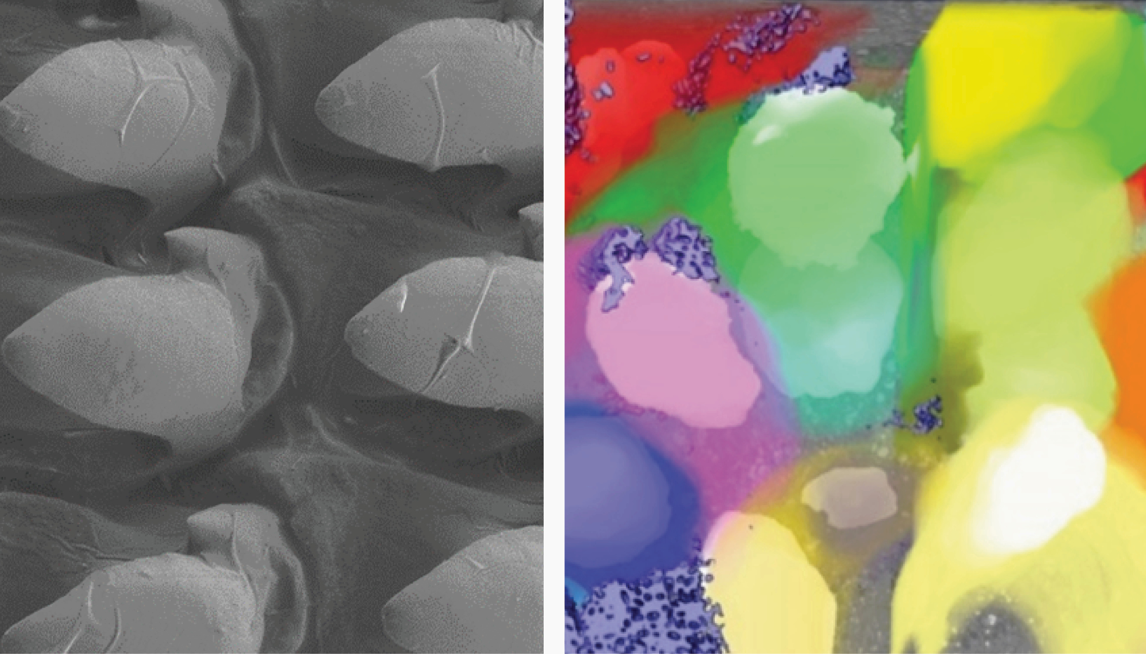
Electron microscopy is a powerful tool for topological, morphological and chemical analysis of a broad range of samples. These data range from determining the elemental composition of certain materials to the 3D rendering of specific structures of interest in biological tissue samples. In combination with other imaging modalities, SEM offers the perfect platform for precision analysis in both the material and biological sciences. Our equipment is housed on both Stellenbosch and Tygerberg campuses.
For more information about an instrument, click on the name of the instrument:
|
Zeiss Merlin FEG SEM
Location: Chamber of Mines Building - Voltage of 100V to 30kV and beam currents of 90nA to 1,4 nA
- Resolutions down to 0.6 nm at 30kV and 1.6 nm at 1kV
- Software: SmartSEM and Aztec/INCA Oxford
- Detectors:
- SE (In-lens & SE2) - nano & micron scale imaging
- BSE (BSE1 inlens & BSE2 retractable) - nano-BSE & 5-diode detector nano to micron imaging
- STEM - (5 diode) sub-nano imaging
- Cathodoluminescence (CL) imaging
- EDX (mapping, LAM, spot, cryo-stage, feature & automate analysis)
|
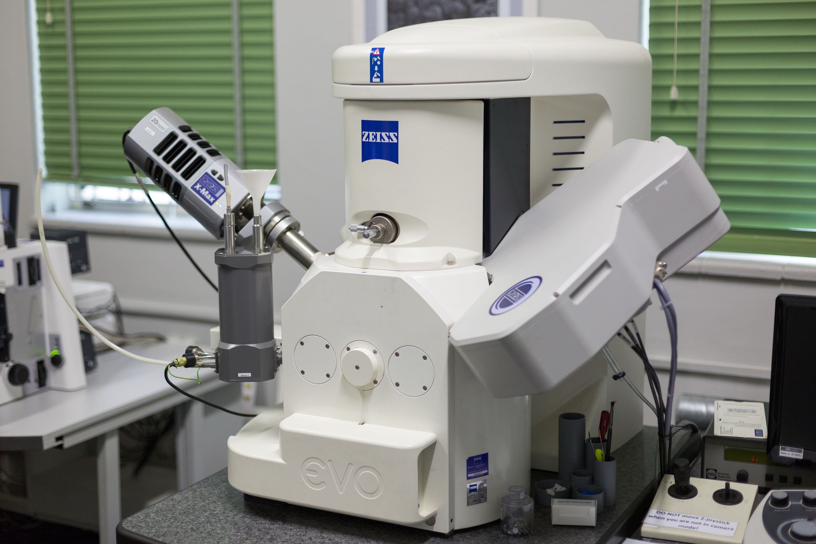
| Zeiss EVO MA 15 EDS/WDS SEM
Location: Chamber of Mines Building
- Voltage of 5kV to 30kV and beam currents of 100 μm to 1,1 nA
- Resolutions down to 0.6 μm at 30kV and 1.6 μm at 5kV
- Software: SmartSEM and INCA Oxford
- Capable of identifying and quantifying all elements in the periodic table except H, He, Be and Li
- Detection limits ranging from ±0.05 to 0.1 wt.% on the major elements using EDS, and 10 to 100ppm on trace elements using WDS
- quantitative analysis, errors ranging from ± 0.5 to 0.01wt% on the major elements using EDS
- Detectors:
- SE - micron scale imaging
- BSE - 5-diode detector micron imaging
- EDS using an Oxford Instruments® XMax 20 mm2 using Oxford INCA software
- Wave Dispersive X-ray Spectrometer using Oxford INCA software
- EDX/WDS (mapping, LAM, spot, montage mapping, feature & automate analysis)
- EDS/WDS quantitative analyses accelerating voltage 20kV, IProbe 1.1nA, and specimen current of 19nA and 8.5 mm working distance
|
|
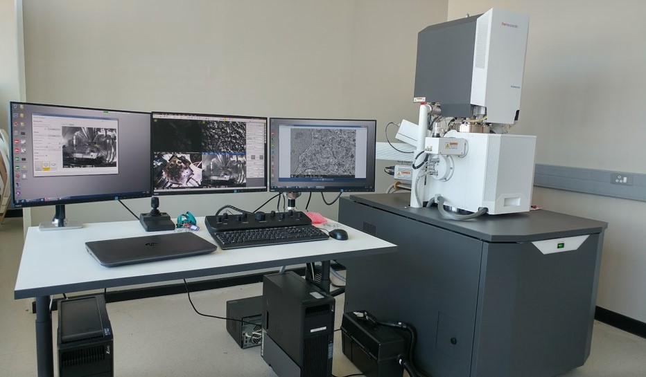
ThermoFisher Apreo Serial Block Face FESEM
Location: BMRI SOUTH, Room 2106
- Voltage range of 200 V – 30 kV and beam current of 1 pA to 400 nA
- Resolution down to 0.8 nm at 30kV and 1.3 at 1kV
- Software: XtUI, MAPS, AMIRA
- Detectors:
SE: T1 & T2 in-lens detectors and ETD (Everhardt-Thornley) BSE: Retractable Directional Backscattered (DBS) LVD: Low Vacuum Detector, up to 0.5 mbar
- T1 segmented lower in-lens detector - VS-DBS: Low Vacuum lens-mounted BSED 2. Cutting thickness: 50nm – 10nm (requires multi energy deconvolution for 10nm) 3. Cutting speed: 0.1 – 0.5 mm/sec 4. Sample Z travel range: 1.2 mm |
